Version 9.0.0 Released
The KiCad project is proud to announce the release of the next major version of KiCad. Version 9 is packed with new features, improvements, and hundreds of bug fixes. We hope you enjoy the new version! Head to the KiCad download page to get your copy of the new version (note that some packages may still be in the process of being released at the time this announcement is published). Our thanks go out to everyone who contributed to KiCad this past year. Whether your contribution was large or small, writing code, submitting bug reports, improving our libraries and documentation, or just supporting us financially: your help made a difference.
In accordance with the KiCad stable release policy, version 8 of KiCad will no longer be actively maintained, and we will release bug fix versions of KiCad 9.x over the next year as we develop new features for KiCad 10. Read on to see some of the highlights of the new version!
Version 9 Changes
Most, if not all, of the new features as well as usability improvements in KiCad 9 are described in a running thread on the KiCad user forum. This thread is being kept reasonably up to date so users running nightly builds know about new features to take for a test spin and provide bug reports and feedback. Wayne Stambaugh also presented them in his FOSDEM 2025 talk which is available to watch on the FOSDEM website. This post highlights some of the major changes, but is not a complete list. There were also hundreds of bug fixes, performance improvements, and other smaller changes since KiCad 8. A full list of issues addressed in KiCad 9 can be found on the milestone page on GitLab.
By the Numbers
Source repository contributions
KiCad 9 was built with changes and additions from hundreds of developers, translators, library contributors, and documentation submitters. There were 4,870 unique commits made that changed code and translations, which was roughly equivalent to Version 8. Our annual development cycle continues to provide regular major releases for our user base and attract new contributors and sponsors.
Improvements to the official KiCad libraries
2024 was another big year for the KiCad library team. With the help of six new librarians joining the effort, the library gained almost 1500 new symbols, 750 new footprints, and 132 new 3D models along with thousands of updates to fix or improve existing parts. The team processed over 2309 merge requests. With even more people helping this year, the team is able to address issues more quickly and has been driving down the backlog of pending merge requests. We are excited to see so many contributors join the library team and accelerate the library’s growth.
General
Jobsets (predefined output jobs)
Mark Roszko contributed a feature that provides predefined sets of ‘jobs’—for example, plotting, exporting, and running DRC—on schematics and PCBs. Independent jobset files are reusable as users may want to create output pipelines that they can apply across their projects for consistency. Jobsets can be run from the command line or from the KiCad GUI.
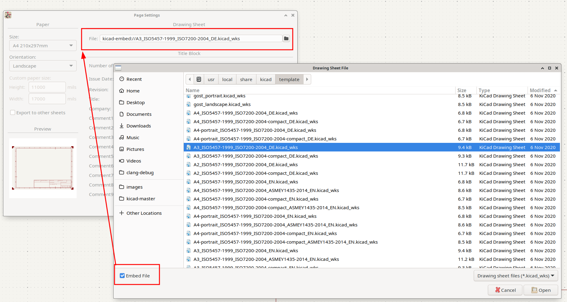
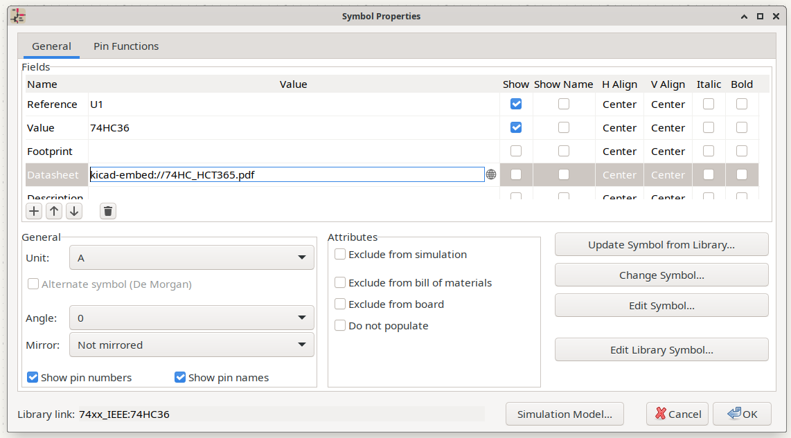
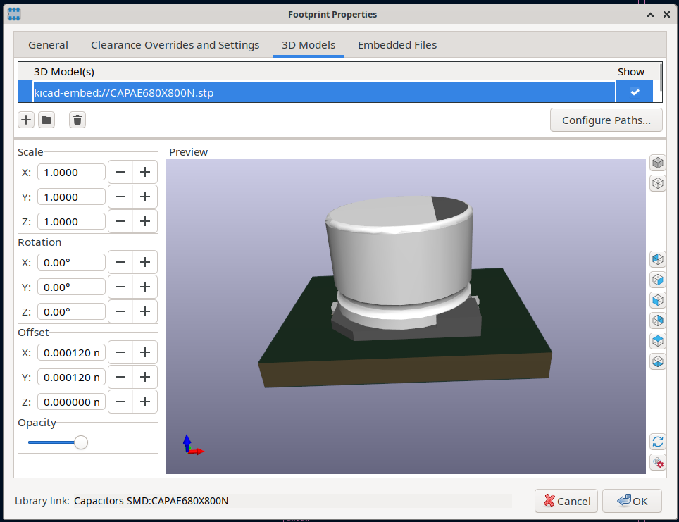
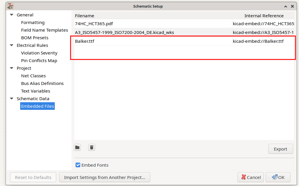
Embedded files
Seth Hillbrand implemented embedding various elements in your schematics, PCB layouts, footprints and symbols that were previously linked to external files. This allows the creation of fully self-contained KiCad files that do not rely on any external files such as fonts or 3D models.
Bezier curve tool in all editors
A Bezier curve creation tool in the schematic and PCB editors was implemented by John Beard. Like the arc tool, there are some guide lines in the PCB editor and by default it chains them as tangent to each other. The backspace key works in the same way as the arc tool. The interactive edit guides are not (yet) in the schematic editor (same for arcs). Beziers were already importable and editable once imported, but now they can be created from scratch.
Multi-channel design support
Tomasz Wlostowski contributed support for creating multi-channel designs. This allows the user to repeat PCB layout elements from one channel to create identical copies.
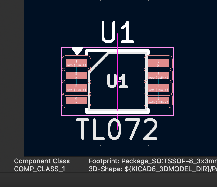
Component classes
James Jackson has added a component class feature that allows grouping of various symbols and footprints into classes that can have specific design rules applied. Component classes are set on symbol in the schematic editor and then apply to the footprints associated with those symbols. Directive labels attached to a rule area can now take a ‘Component Class’ field. Symbols within the rule area will be assigned that component class. The ‘Component Class’ field can be set directly on symbols as well:
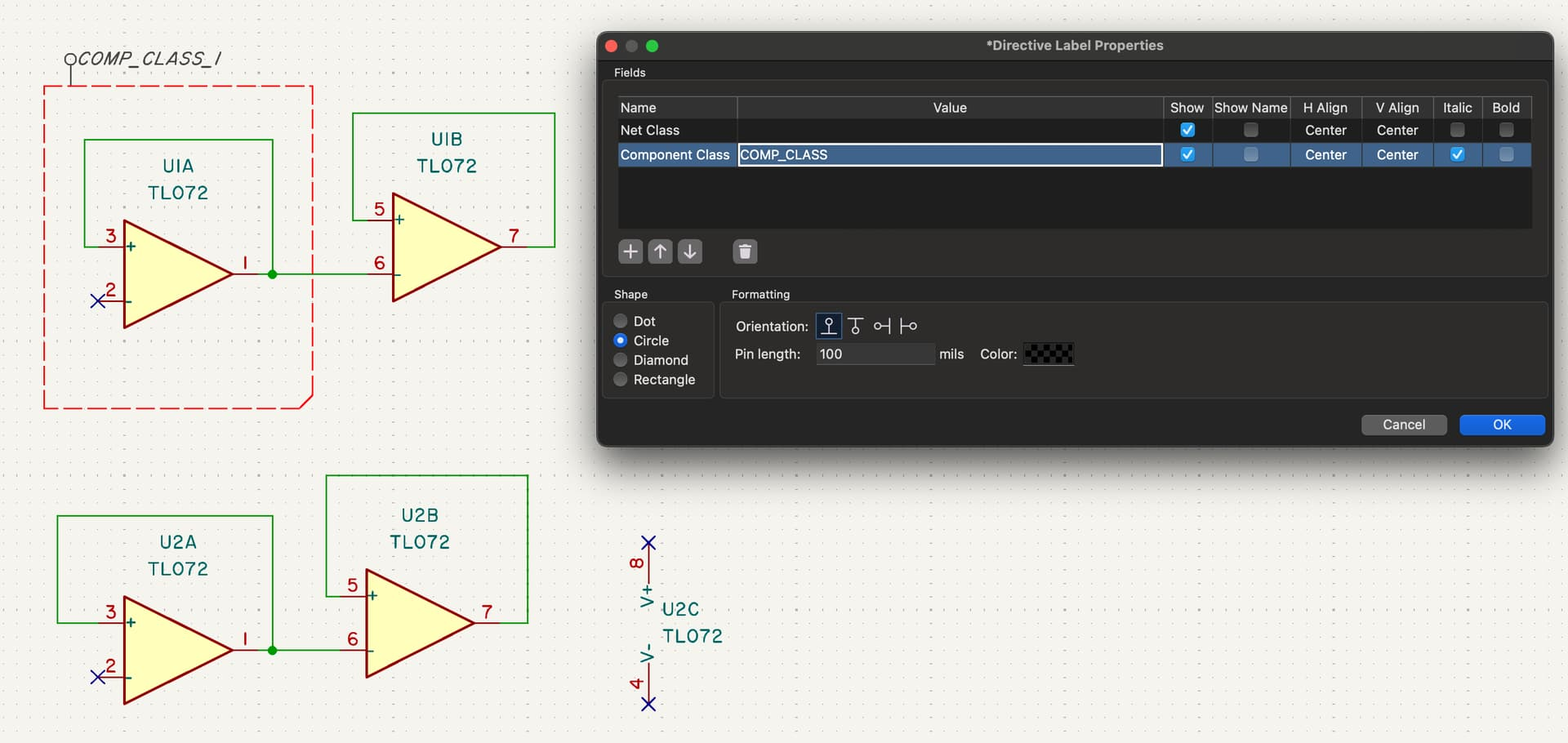
Symbols can have more than one component class, taking on any that are defined directly on the symbol or any of its sub-units or from any directive labels attached to any rule areas which contain the symbol.
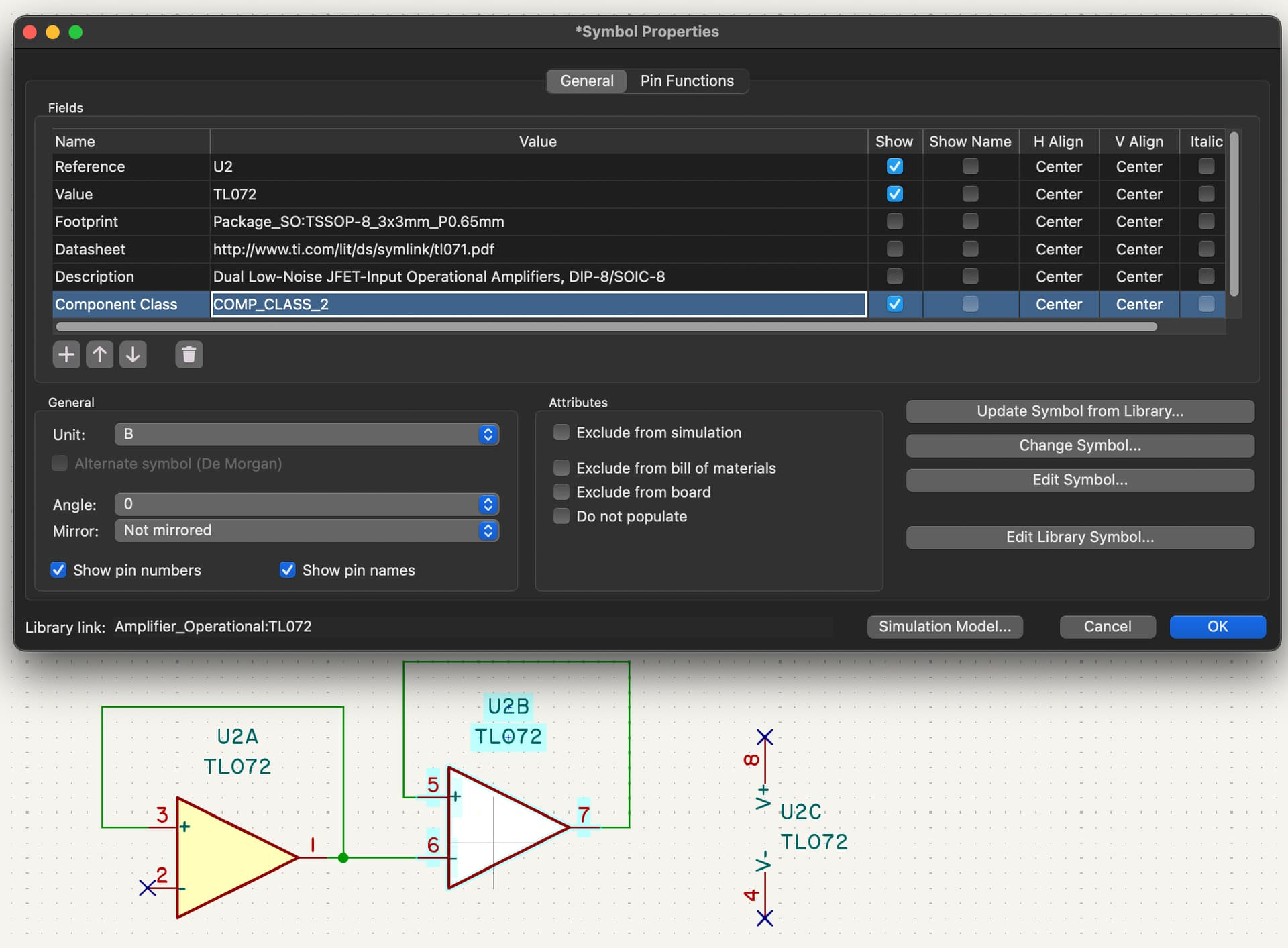
In the PCB editor, component classes are attached to the symbol’s footprint:
There are three new DRC expressions / functions to support querying component classes:
(condition "A.ComponentClass == 'CLASS_1,CLASS_2'")to test against the full list of component classes, where the composite component class is a comma-delimited list in alphabetical order),
(condition "A.hasComponentClass('CLASS_1')")to test if a footprint is part of a specific component class, and
(condition "A.memberOfFootprint('${Class:CLASS_1}')")to test if an item is part of a footprint in a specific component class.
Table editing in schematic, symbol, and footprint editors
Thanks to the efforts of Jeff Young, tables can now be added to schematic, symbol library, and footprint library editors putting them on par with the PCB editor. Additional editing features were also added to tables.
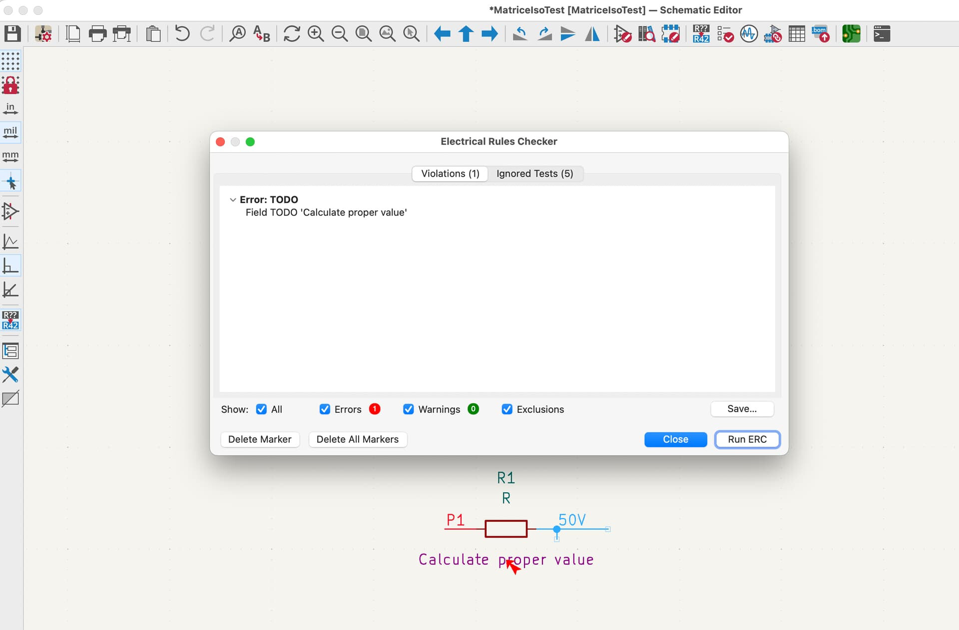
Custom ERC/DRC errors, warnings, and exclusion comments
Jeff Young added a feature that lets you create ERC/DRC errors and warnings from text boxes and fields using the following text variables:
${ERC_WARNING <custom title>}
${ERC_ERROR <custom title>}
${DRC_WARNING <custom title>}
${DRC_ERROR <custom title>}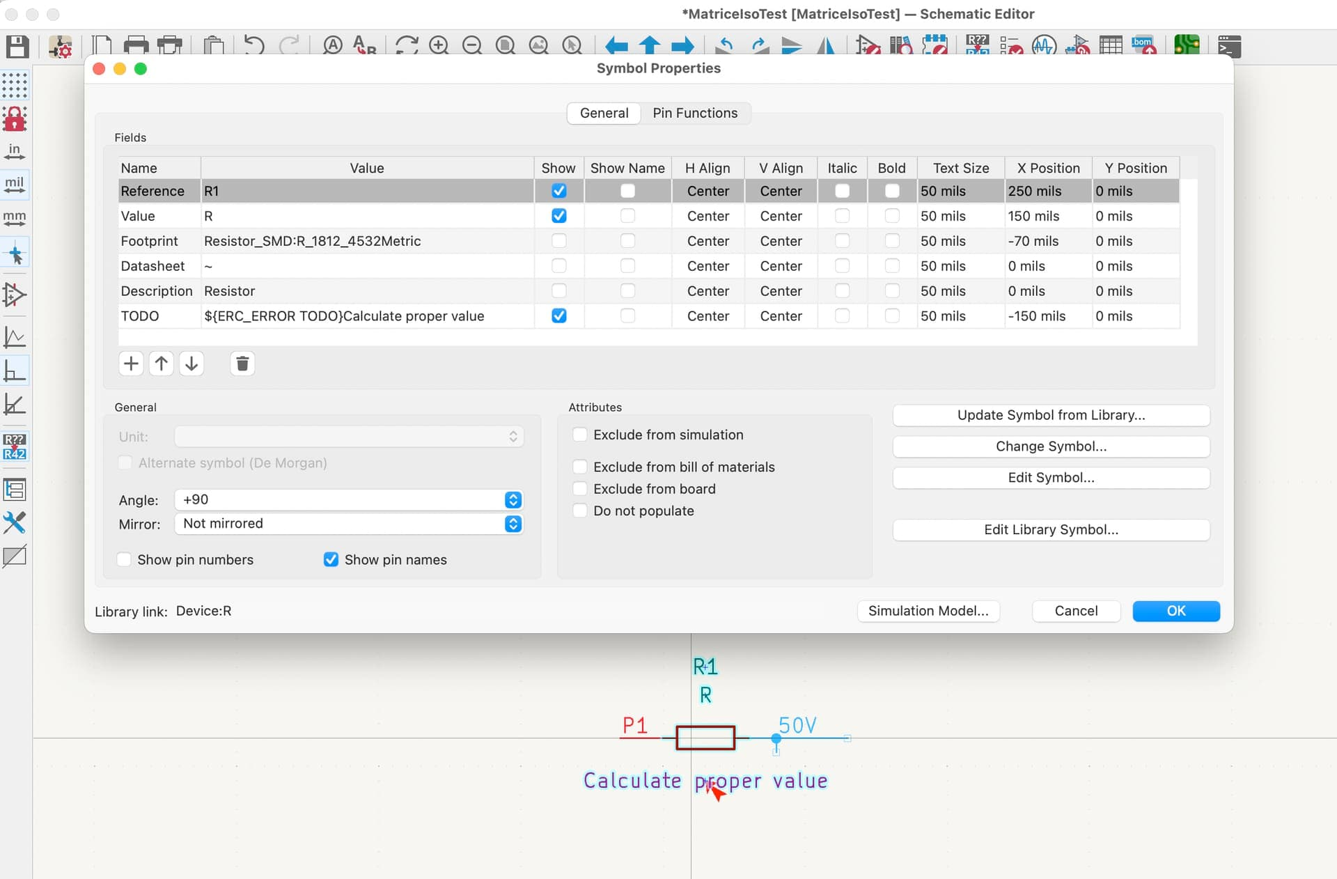
Mouse scroll wheel actions
John Beard added a scroll action feature in the PCB, schematic, footprint and symbol editors. Shift-Alt-Scroll is a primary function and Ctrl-Alt-Scroll is a secondary function.
The current bindings are to use this to increment text, with the rightmost “part” being primary and the next rightmost part being secondary. For example, Shift-Alt-Scroll on “B2” goes to “B1” or “B3”, Ctrl-Alt-Scroll goes to “A2” or “C2”. This is a bit heuristic, but seems to work well for the obvious cases. As a side effect of being able to detect the mouse being over name or number, the symbol editor “Edit Pin” dialog now puts the initial focus on the number field if the mouse was over it when double-clicked or the ‘E’ hot key.
-
Footprint editor: pad numbers and text
-
PCB editor: text
-
Symbol editor: pin numbers or names (depending on mouse position) and text
-
Schematic editor: labels and text
Continued Documentation Improvements
Graham Keeth has been hard at work updating KiCad’s documentation for Version 9. Thanks to his work, most of the new features and changes in KiCad 9 are already documented. In addition to documenting new features, Graham has been improving all areas of the documentation with updated screenshots, copy editing, and corrections. Our documentation translators have also been working to update the translated text so that up-to-date KiCad documentation is available in more languages.
Other KiCad-wide changes
-
The command line interface gained several new abilities, including raytracing 3D images
-
Reverse mouse wheel zoom option
-
Image reference points
-
Expand/collapse all context menu entry in library editor tree panels
-
Assign multiple net classes to a net
-
Context menu copy from inspector report panels
-
Text justify actions that can be mapped to hot keys
-
Comment can be added to ERC/DRC exclusions
-
Right-click action to remove ignored tests from the ERC/DRC dialogs
-
Right-click copy of inspector window contents.
-
Allow pasting images from the clipboard as reference images in schematic, PCB, and worksheet editors
-
"Copy as Text" action which allows copying the text content of text items, fields, labels, tables, table cells, and dimensions
Schematic and Symbol Editors
Selection filtering
The schematic and symbol library editors now have object selection filtering like the PCB and footprint library editors have thanks to Jon Evans.
Sheet pin/hierarchical label synchronization tool
One of our newest core team developers Ethan Chien has contributed a new sheet pin/hierarchical label synchronization tool. This tool provides management of sheet pins and their associated hierarchical labels instead of having to switch back and forth between the sheet and schematic.
Net class rule areas
James Jackson added support for schematic net class rule areas that allow users to draw a shape to which net class directives can be attached to all nets defined by the shape.
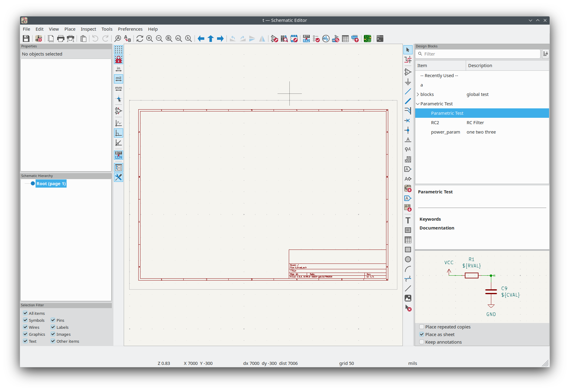
Design blocks
Mike Williams contributed the schematic design blocks implementation. This feature allows users to create libraries of reusable schematic blocks. This feature will be extended to include reusable PCB layout blocks in a future version of KiCad.
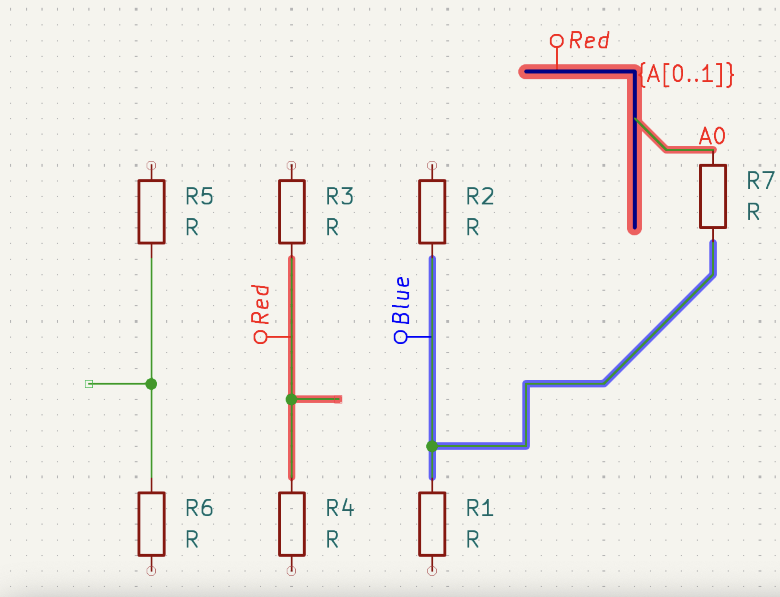
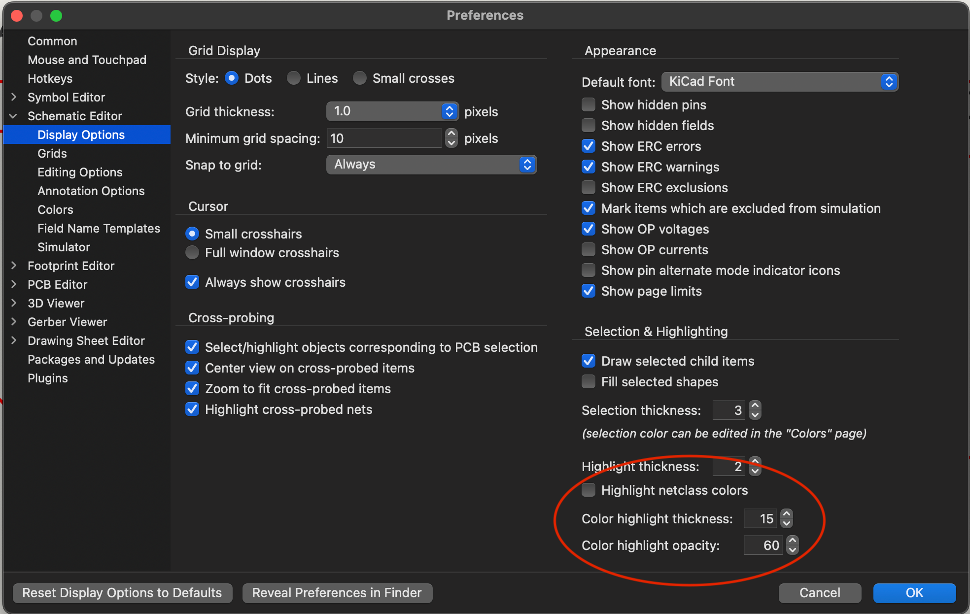
Net class color highlighting
There is a new option to apply net class coloring as a "highlight" around the wire instead of just changing the color of the wire itself. This handy usability improvement was contributed by James Jackson.
Other smaller changes to the schematic editor
-
Saving a symbol to another library in the symbol editor will now save all symbols it is derived from
-
"Save As" and "Save Copy As" commands in symbol editor
-
Warning when attempting to edit read only library with option to make an editable copy
-
Option to not show hidden fields in the symbol editor
-
Net navigator now displays all nets in the schematic
-
Option to exclude symbols from simulation
-
Import Eagle schematics with modules
-
Symbol editor pin dragging
-
Symbol alternate pin mode indicators
-
Save derived symbols to different library
-
ERC for local and global labels with the same name
-
ERC for unconnected endpoints
-
Support importing Altium ASCII schematic file format
-
Sheets can be renamed from the hierarchy navigator
-
Option to exclude symbols from simulation
-
Option to show indicators on symbol pins with alternate definitions
-
Ability to mark an entire sheet as "do not populate", "exclude from board/BOM", or "exclude from simulation"
-
Option to plot the "do not populate" indicators
-
Allow changing symbol unit in "Edit Reference Field" dialog
-
Allow assigning multiple net classes to a single net
-
Introduces ordering of net classes
-
Allow net classes to have null properties (except default net class)
-
Effective net classes are constructed from non-null net class fields in net class priority order with default net class parameters always used as fallback
-
DRC checks for net class equivalence as requiring both items to have the same set of constituent net classes
-
DRC test net class name
(A.netclass == 'my_netclass')against the comma-separated list of priority ordered constituent net classes -
Add DRC function
A.hasNetclass('my_netclass')to test if a given net class is assigned to an item -
Schematic and PCB net class coloring taken from the effective aggregate net class for a net
-
PCB and Footprint Editors
IPC API
Jon Evans created a new API for the board editor based around inter-process communication (IPC) that will eventually replace the current Python wrapper interface. This interface will provide much improved stability and API stability over the wrapper interface and will be extended to support the schematic editor during version 10 development. For more information on the new API, please see the developer documentation.
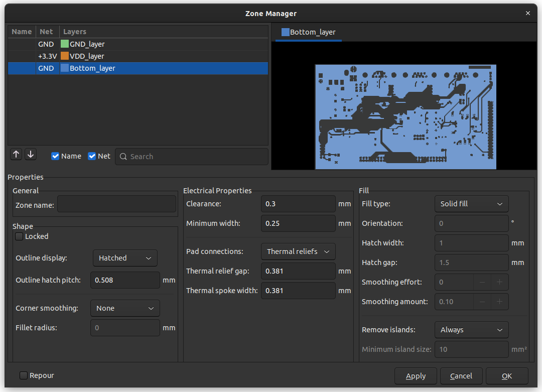
Zone manager
Ethan Chien has contributed a new zone manager feature which allows easy preview and adjustment of zone priorities and other settings without having to edit each zone individually to verify the result of the changes.
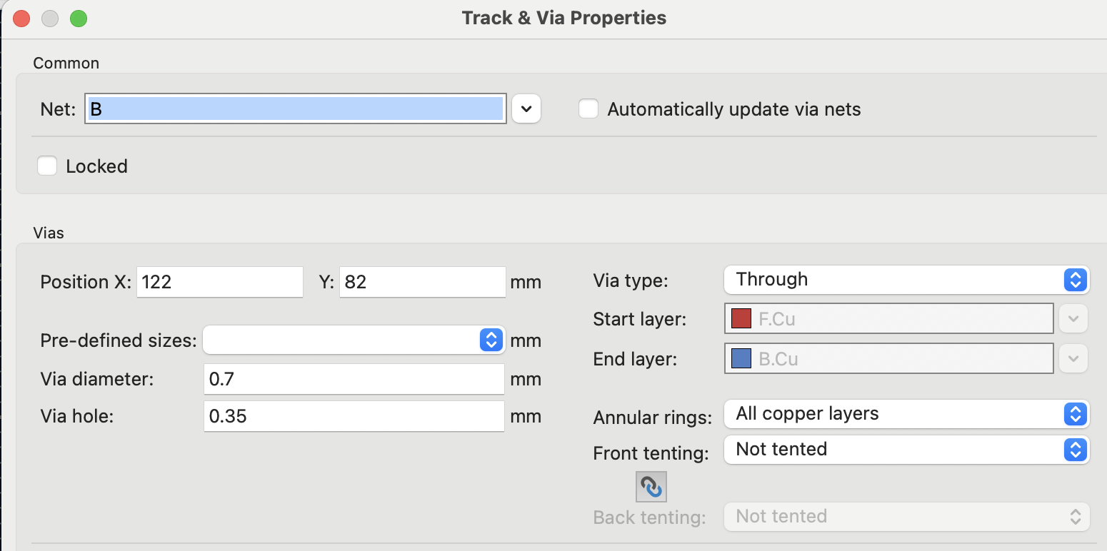
Improved via tenting control
Control over via tenting on top and bottom sides at a board level and per-via overrides was provided by Jon Evans. This change allows complete control over via tenting compared to the options available in previous versions of KiCad.
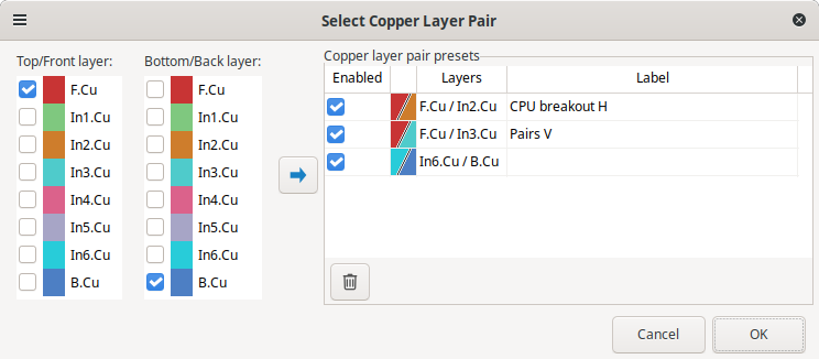
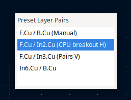
Layer pair presets
John Beard added some helpful features for working with layer pairs: presets and a quick-switch list. “Enabled” pairs, along with the currently-set pair if not itself a preset, can be cycled with the “Shift+V” hot key.
Shape modification tool
Internal board cutouts usually cannot be manufactured with sharp corners. John Beard created an aptly-named "Dog bone" tool to create the proper shape(s) determined by the diameter of the tool used to route the cutout.
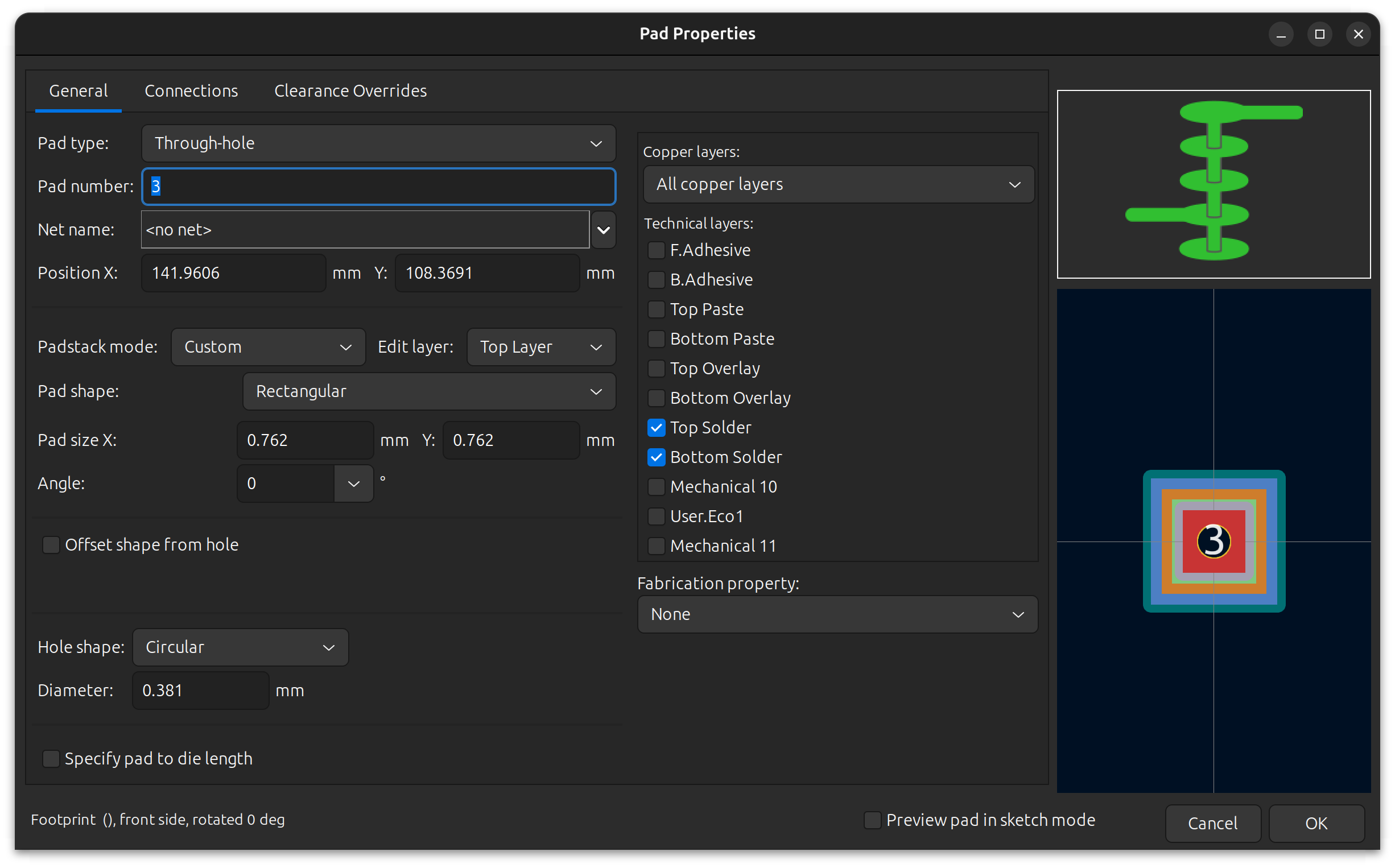
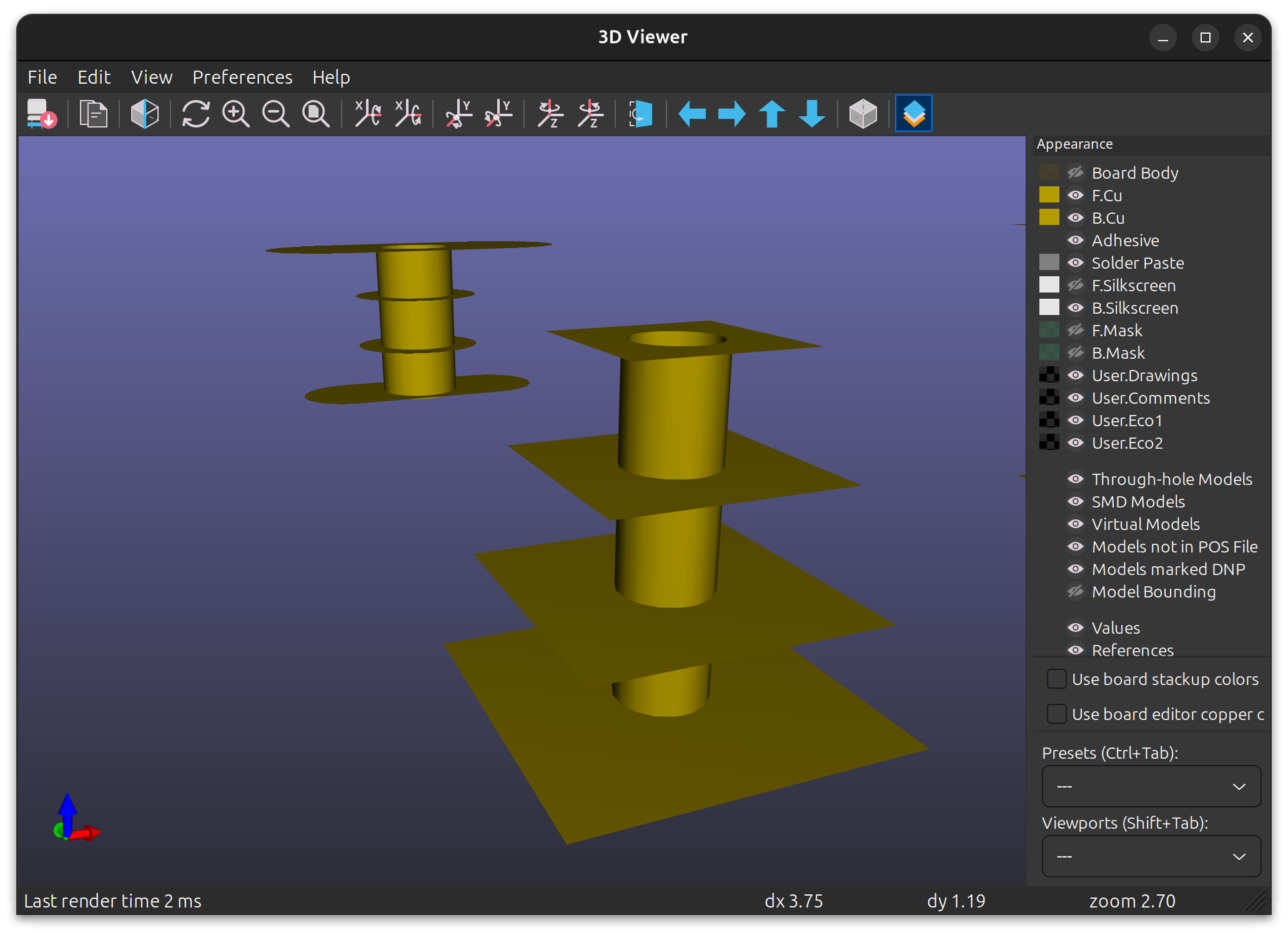
Pad stacks
Thanks to the efforts of Jon Evans, KiCad now supports PTH pads with different copper shapes on different layers. Pad stacks can be defined with different shapes on the top, inner, and bottom layers, or with unique shapes on every copper layer.
Interactive positioning tool
Another handy tool by John Beard allows users to position objects by drawing a line and then defining what that line should be.
Another use is a more direct way to manipulate objects by first getting them into a known position and then using Move Exact. It can also be used to set alignment in one axis or the other.
The vector doesn’t have to be on either object, which allows direct use of a dimension of something else as a movement for the selection.
Multiple track drag
Tomasz Wlostowski updated the push and shove router to allow dragging of multiple tracks. While not the same as routing multiple tracks, this change will greatly improve routing boards with complex buses.
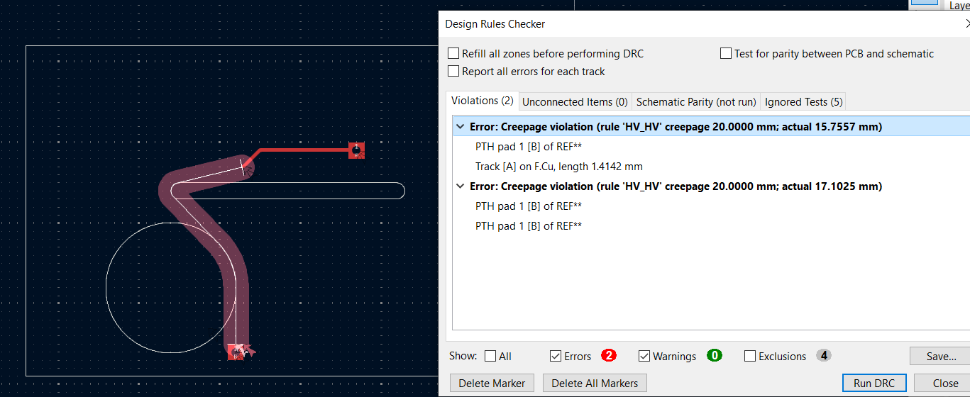
Creepage design rule check
Fabien Corona implemented a design rule check for electrical creepage clearances. The new rule syntax and the resulting DRC errors are shown below.
(rule HV_HV
   (constraint creepage (min 20mm))
   (condition "A.hasNetclass('A') && B.hasNetclass('B')")
)
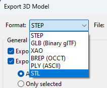
3D model export improvements
3D models can now be exported to XAO, STL, BREP, and PLY file formats including silk screen and solder mask layers thanks to the efforts of Aleksandr Shvartzkop.
Other changes to the PCB editor
-
Net inspector panel
-
Cursor snap indicators
-
ODB++ export
-
Option to plot pad outlines and numbers on fabrication layers
-
Allow pasting text directly as text items
-
Include silk screen and solder mask in 3D export
-
Filter models to include/exclude in 3D export
-
Plot all layers to a single PDF document with separate pages instead of to separate PDF files per layer
-
Differential pair skew and acute angle design rule checks
-
Optional skew DRC flag for independently checking differential pair skew rules
-
Design rule failure clearance indicators
-
Track solder mask removal
-
Arbitrary reference for relative position tool
-
Cursor snap indicators
-
External dimension leaders
-
Zone corner chamfering
-
Option in position relative tool to use arbitrary reference point which can be snapped to objects
-
Outset creation tool
-
Polygon simplification tool
-
Vias with per layer diameter annular rings
-
Override locked footprints when updating PCB from schematic
-
Allowing grouping of user defined layers as front/back pairs
-
Exporting 3D models from command line interface with ray tracing is now supported
-
Extend
physical_clearancerule to apply between copper fills and footprint courtyards -
Improved rendering of plated through holes
-
Inward facing dimension arrows
-
3D model export improvements
-
Option to fuse copper geometry together
-
Option to export copper on inner layers
-
Options to exclude board body or footprint models
-
Net filter (can be used to export a single net)
-
Zone geometry approximation with arcs for faster processing and smaller file sizes
-
Other tools
-
Tolerance calculations added to calculator tool regulator panel
See Also
KiCad 8.0.9 Release
2025-02-19
The KiCad project is proud to announce the version 8.0.9 bug fix release. The 8.0.9 stable version contains critical bug fixes and other minor improvements since the previous release.
KiCad Version 8.0.9 Release Candidate 1 Available
2025-02-16
The first release candidate for version 8.0.9 is available for testing. Version 8.0.9 will be released soon unless critical issues are found in testing this release candidate. This will most likely be the final 8.0 series bug fix release with the release of the 9.0 series is happening soon. There may be additional bug fixes to the 8.0 series available as testing builds for users who require those bugs fixed after 8.